NV Center ODMR Unlocks New Possibilities for 2D Materials and Spin Wave Detection
In short
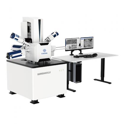
Three research teams used CIQTEK ODMR instruments, including the scanning NV probe microscope (SNVM) and the diamond single-spin spectrometer, to move three different areas of advanced materials research forward.
A team at the Institute of Physics, Chinese Academy of Sciences, imaged spin waves in real space near magnetic defects and antiferromagnetically coupled stripe domains in YIG and LSMO films. They captured wavelength-selective scattering and, for the first time, a zig-zag wavefront distortion as spin waves crossed stripe domains.
A team at the University of Science and Technology of China stripped selenium out of 2D CuCrSe₂ by vacuum annealing. The resulting Se vacancies produced room-temperature ferromagnetism while the layered crystal structure stayed intact.
A team at the Institute of Semiconductors, Chinese Academy of Sciences, mapped how a transverse magnetic field mixes NV center spin states, weakens optical readout, and shifts the balance between the NV⁻ and NV⁰ charge states, all of which matter for keeping NV-based sensors stable in real-world magnetic environments.
Why this matters
Optically detected magnetic resonance (ODMR) sits at the center of solid-state spin science. It is how researchers image microscopic magnetic fields, how they unpack spin dynamics, and how they turn a single atomic-scale defect in diamond into a working sensor. The three studies below all leaned on CIQTEK's ODMR product line, which includes the scanning NV probe microscope (SNVM) and the diamond single-spin spectrometer, to push into territory that older tools could not reach: spin wave imaging, room-temperature ferromagnetism in 2D materials, and the spin mixing behavior of NV centers themselves.
Here is what each team found, and why it matters for anyone building magnonic devices, spintronic materials, or diamond-based sensors.
Where it was published: SCIENCE CHINA Physics, Mechanics & Astronomy
Paper title: Visualizing modified spin-wave wavefronts near magnetic defects and domains using nitrogen-vacancy centers
Research group: The Li Yangmu group at the Institute of Physics, Chinese Academy of Sciences
The team used scanning NV imaging to perform real-space imaging and phase analysis of spin wave propagation and wavefronts near nanoscale magnetic defects and antiferromagnetically coupled stripe domains in magnetic thin films (YIG and LSMO). The work revealed wavelength-selective scattering and waveform modulation, giving device designers a new set of tools for building and tuning spin wave devices.
First, some background: why spin waves are hard to see
Spin waves, also called magnons, are collective excitations of a magnetically ordered system. They carry information without the Joule heating losses that come with conventional charge-based devices, which makes them an attractive carrier for low-power, wave-based information computing.
The problem is scale. Inside complex magnetic structures at the nanometer level, the scattering of spin waves and the evolution of their phase have been very difficult to observe directly in real space. Existing characterization methods all have limits: Brillouin light scattering, scanning transmission X-ray microscopy, and time-resolved magneto-optical Kerr effect each fall short in their own way.
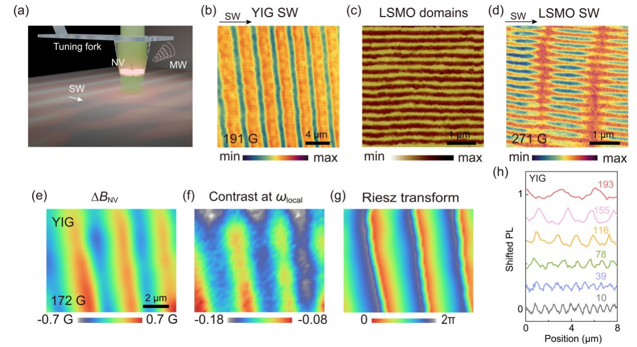
NV centers offer a complementary route. They can detect magnetic textures, spin wave phase, and chirality at the same time, which is exactly the combination needed here. So the team turned to CIQTEK's scanning NV probe microscope (SNVM) and ran real-space spin wave imaging on two representative magnetic thin films: yttrium iron garnet (YIG) and lanthanum strontium manganite (LSMO).

Figure 1: Spin wave and magnetic domain images of YIG and LSMO (measured with the CIQTEK SNVM).
Finding 1: What happens near magnetic point defects in a YIG film
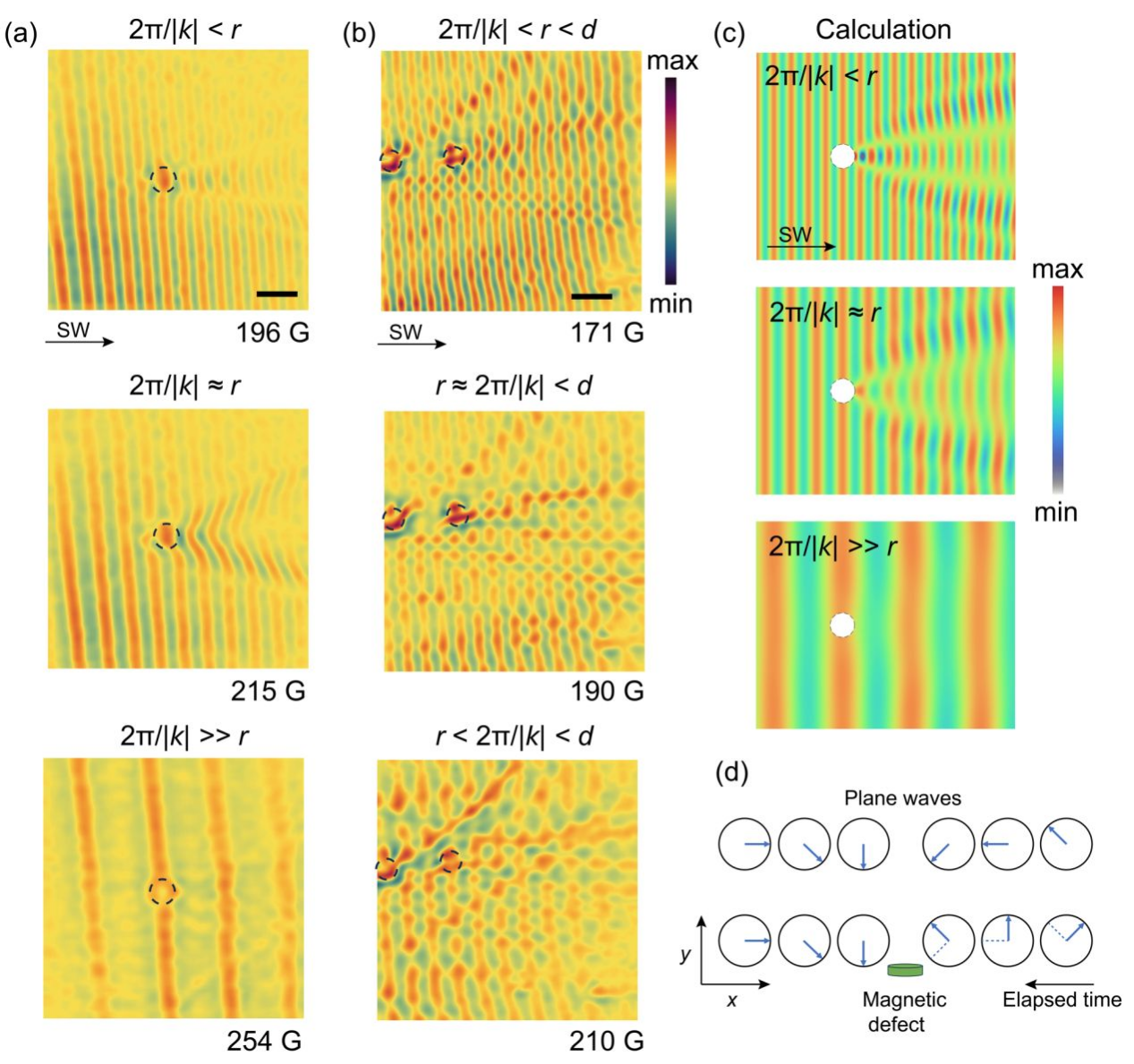
Scattering strength depends on a ratio. Whether a spin wave scatters strongly off a point defect comes down to the relative size of the spin wave wavelength versus the characteristic size of the defect. When the wavelength is close to the defect size, the spin wave wavefront bends and distorts noticeably. When the wavelength is much larger than the defect size, the spin wave passes through with almost no disturbance at all.
Multiple defects create interference. When a spin wave interacts with several point defects at once, it produces the classic wave interference pattern.
Experiment and theory line up. The magnetic defect behaves like a secondary radiation source that emits cylindrical scattered waves. The total phase shift near the defect is set by the amplitudes of both the incident and the scattered wave, and the theoretical model reproduces the scattering features seen in the experiment.

Figure 2: Spin wave images near a magnetic point scatterer in a YIG film.
Finding 2: What happens near magnetic domain structures in an LSMO film
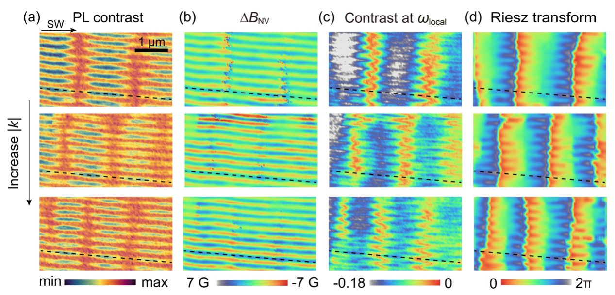
A first. The team experimentally observed, for the first time, spin waves taking on a zig-zag wavefront distortion as they crossed stripe domains.
Why the zig-zag appears. Adjacent magnetic domains have opposite equilibrium magnetization directions. That forces the direction of the phase gradient to flip between neighboring domains, so that both phase continuity near the boundary and the dispersion relation are satisfied at the same time.
What the simulations showed. Micromagnetic simulation analysis found that the dynamic magnetization component mx keeps the same sign across adjacent domains, while the my component reverses sign. The mx component is mainly concentrated near the domain walls. A local magnetic field difference of roughly ±7 G between adjacent domains causes a shift in the local NV resonance frequency.

Figure 3: Non-degenerate state measurement of antiferromagnetically coupled stripe domains and spin waves in LSMO.
Why this study stands out
Unlike traditional methods that rely on magnetic field inversion, the CIQTEK scanning NV probe microscope enabled simultaneous in-situ measurement of spin wave phase and static magnetic domains. That combination opens a new way to study how magnetic defects, domain boundaries, and spin waves interact with one another, and it gives magnonic device development a new experimental tool.
Where it was published: SCIENCE CHINA Materials
Paper title: Anion modulation induced room-temperature ferromagnetism in two-dimensional CuCrSe₂
Research group: The Wu Changzheng team at the University of Science and Technology of China
This team proposed an "anion modulation" strategy. By selectively removing Se anions from CuCrSe₂ through vacuum annealing, they introduced Se vacancies inside the material.
Pulling selenium out, without breaking the crystal
The numbers here are worth pausing on. After 20 minutes of annealing, the Se loss ratio in the CuCrSe₂ nanosheets was about 10%, yet the material kept its original layered crystal structure. There was no obvious structural phase transition and no second phase. Multiple structural characterizations together confirmed that the annealing process mainly caused the removal of Se anions.
Confirming magnetism at room temperature
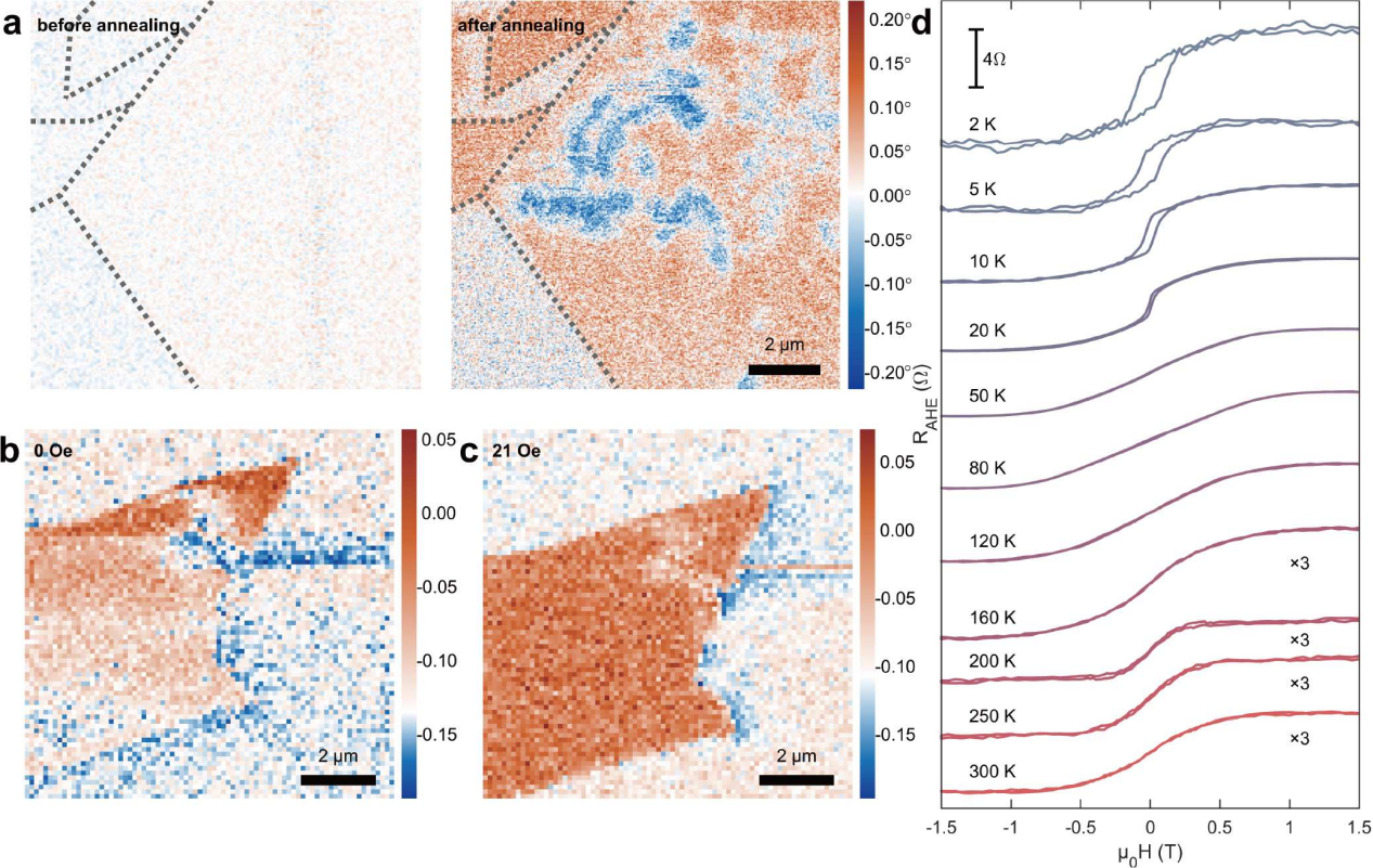
To verify that the material was ferromagnetic at room temperature, the team combined several techniques: magnetic force microscopy (MFM), the scanning NV probe microscope (SNVM), and anomalous Hall effect (AHE) measurements. Among them, the SNVM results clearly showed a local magnetic signal in the annealed CuCrSe₂ nanosheets at room temperature, while the samples that had not been annealed showed no obvious magnetic domains.

Figure 4: Room-temperature ferromagnetism testing of A-CuCrSe₂ material.
What is happening at the atomic level
Theoretical calculations revealed the microscopic mechanism behind the enhanced magnetism. Se vacancies at specific sites can change the magnetic moment distribution of the surrounding Cr atoms, produce a more pronounced magnetic moment splitting between Cr atoms, and narrow the spin-orbit exchange energy gap, which strengthens the ferromagnetic superexchange interaction between Cr and Cr.
The position of the vacancy matters. Se vacancies at different positions have noticeably different effects on magnetism, and the Se vacancies at the advantageous sites are the key to achieving high-temperature ferromagnetism.
Why this study stands out
The work shows that selectively tuning anion vacancies in 2D materials can effectively strengthen magnetic interactions while preserving the original crystal structure. That points to a new route for making room-temperature 2D ferromagnetic materials, and it offers an important reference point for designing low-dimensional magnetic materials aimed at spintronics.
Where it was published: ACS Photonics
Paper title: Optically Detected Spin Mixing of Nitrogen-Vacancy Centers in Diamond
Research group: The Zhang Jun research team at the Institute of Semiconductors, Chinese Academy of Sciences
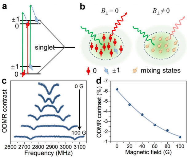
This study systematically revealed the spin mixing, optical readout degradation, and charge state conversion mechanisms of diamond nitrogen-vacancy (NV) centers under a transverse magnetic field. The results offer a new way to improve how stable NV-based sensors stay when they operate in complex magnetic environments.
The problem with a field that will not line up
Diamond NV centers are an important class of solid-state quantum defects. They can be initialized by laser, manipulated with microwaves, and read out through fluorescence, which is why they have been widely used in high-sensitivity magnetic field measurement, quantum imaging, and quantum information processing.
In a real device, though, the applied magnetic field rarely aligns perfectly with the NV axis. When the field has a transverse component, it mixes the different spin sublevels of the NV center and weakens the ability to optically polarize the spins, which in turn affects fluorescence readout and magnetic resonance signals.
What the team measured
The researchers used CIQTEK's ODMR-related instruments together with photoluminescence (PL) and continuous-wave optically detected magnetic resonance (ODMR) techniques to systematically measure how diamond NV centers respond under different magnetic fields and temperatures.
ODMR works by monitoring the fluorescence changes caused by microwave-driven spin transitions, which reflects how well the NV center can initialize its spin and how well the optical readout performs. The experiments found that as the transverse magnetic field grows stronger, the ms=0 and ms=1 spin states of the NV center mix more noticeably. Optical polarization efficiency drops, and ODMR contrast weakens along with it.

Figure 5: Measuring the spin mixing effect of NV⁻ under a transverse magnetic field using ODMR.
The critical magnetic field Bc
To quantitatively evaluate how well an NV center tolerates a transverse magnetic field, the team extracted a critical magnetic field, Bc, from the field-dependent PL contrast curves. This parameter marks the field scale at which spin mixing starts to significantly affect optical readout. A larger Bc means the NV center is more stable against transverse magnetic fields. A smaller Bc means its optical readout is more easily disturbed by field misalignment.
Temperature changes the picture
The study also found that the critical magnetic field depends clearly on temperature. In a specific intermediate temperature range, the fluorescence response of the NV center was significantly suppressed.
By building a Lindblad master equation model that includes the excited-state orbital structure, phonon-assisted orbital relaxation, and spin-dependent intersystem crossing, the researchers revealed how temperature changes the excited-state orbital dynamics and, through that, further tunes the spin mixing induced by the transverse magnetic field.
Charge states tell the rest of the story
The team also resolved the zero-phonon line emission of the negatively charged state, NV⁻, and the neutral state, NV⁰, separately. What they saw was that when the transverse magnetic field increased, the drop in NV⁻ fluorescence came along with a corresponding change in NV⁰ fluorescence. In other words, the signal loss caused by the magnetic field does not come entirely from non-radiative processes. It is closely tied to a redistribution between the NV⁻ and NV⁰ charge states.
Why this study stands out
This work ties spin mixing, ODMR contrast decay, temperature effects, and charge state dynamics together into one picture. It proposes an experimental metric that can be used to evaluate the transverse magnetic field stability of NV-based sensors, and it provides important reference points for designing magnetic field direction, optimizing operating temperature, controlling charge states, and improving optical readout performance.
CIQTEK invites you to try the scanning NV probe microscope (SNVM), a world-leading system for nanoscale magnetic field imaging. Key specifications:
Temperature range: 1.8 K to 300 K
Vector magnetic field: 9 / 1 / 1 T
Magnetic spatial resolution: 10 nm
Two configurations are available:
Room-temperature SNVM
Low-temperature SNVM
Try it for yourself: free sample testing and on-site visits
CIQTEK has extensive experience in sample testing and supports on-site visits as well as free sample measurement. If you have a sample you would like tested, email our engineers at sunh@ciqtek.com and we will take it from there.
Want to learn more about our products and how they might fit your work? Reach out any time:
Phone: +86 400-0606-976
Email: gylz@ciqtek.com
What is ODMR?
Optically detected magnetic resonance (ODMR) is a characterization method in solid-state spin science. It works by monitoring the fluorescence changes caused by microwave-driven spin transitions, which makes it useful for microscale magnetic field imaging and for analyzing spin dynamics.
What can a scanning NV probe microscope (SNVM) measure?
SNVM uses NV centers to detect and image magnetic fields at the nanoscale. As the work described above shows, it can measure spin wave phase and static magnetic domains at the same time, which lets researchers study how magnetic defects, domain boundaries, and spin waves interact. The system also supports imaging across a temperature range of 1.8 K to 300 K.
Why is room-temperature ferromagnetism in 2D materials such a big deal?
Because it means magnetism survives without expensive cooling. In the CuCrSe₂ work, selectively removing Se anions through vacuum annealing enhanced the magnetic interactions while keeping the layered crystal structure intact, which points toward practical 2D ferromagnetic materials for spintronics.
Why does transverse magnetic field stability matter for NV-based sensors?
Real devices rarely deliver a magnetic field that lines up perfectly with the NV axis. A transverse component mixes the NV spin sublevels, weakens optical polarization, and reduces ODMR contrast. The critical magnetic field Bc gives engineers a measurable way to compare how well different NV centers hold up under that kind of field misalignment.
Let's keep the conversation going
Follow us for more industry news and research updates from the sensing world. If you would like to see how our ODMR instruments fit into your own work, contact us at gylz@ciqtek.com or call +86 400-0606-976.
No. 1969, Kongquetai Road, High-tech Zone, Hefei, Anhui, China
+8615156059133
+8613083191369
info@ciqtek.com
خريطة الموقع | XML | مدونة | سياسة الخصوصية | شبكة IPv6 مدعومة