ما الذي تبحث عنه؟?
عمليات البحث الشعبية
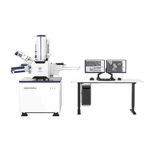
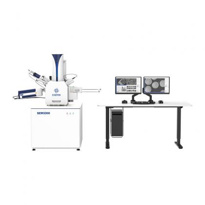
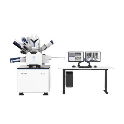
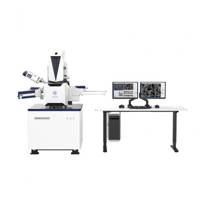
- المورد العالمي للمجهر الإلكتروني لمسح الانبعاثات الميدانية
- أجهزة الكشف SEM EDX، EDS، EBSD، BSE، CL، STEM
- مسح تطبيقات مقياس المغناطيسية NV الكم الماسي ومجهر القوة الذرية QDAFM
- الشركة المصنعة للمجهر المركزي للمسح ciqtek NV
- المسح الضوئي NV المغناطيسية المورد العالمي
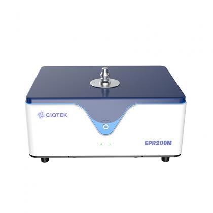
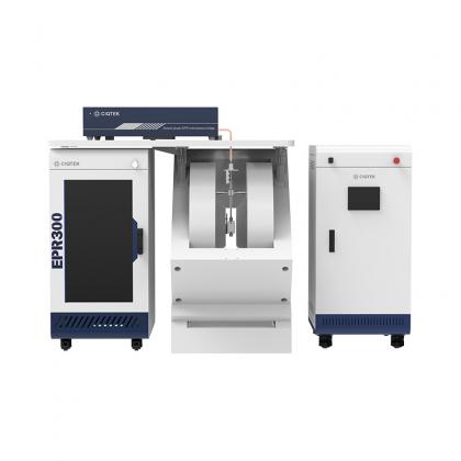
- المورد العالمي لمطيافية الرنين المغناطيسي النبضي X-Band
- التحليل الطيفي بالرنين المغنطيسي الإلكتروني بأفضل الأسعار
- التحليل الطيفي للنطاق X EPR مع ناظم البرد
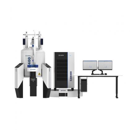
- التحليل الطيفي بالرنين المغنطيسي الإلكتروني ذو النطاق W بأفضل الأسعار
- التحليل الطيفي بالرنين الإلكتروني ذو النطاق W بأفضل الأسعار